Table of Contents
Xilinx Virtual JTAG Cable with USB FTDI chip FT220X
Original document XVC_FT220X02A, UST store
It's a set of software and electronic hardware created by MIHO. It is intended to obtain a more accessible method of programming Xilinx FPGAs. More documents describing this method are available on MLAB documents list page.
Description of solution
To work with Xilinx FPGA it is necessary to use a hardware programmer. It allows a loading of a binary scheme into the chip. This can be realized by connecting the FPGA chip to the JTAG interface device.
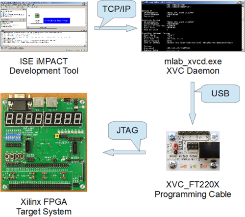
XILINX ISE development suite for FPGAs supports XVC protocol. This protocol allows a remote TCP/IP connection to the JTAG device which is connected to the FPGA chip at the remote end.
Operating principle
This module creates a virtual JTAG cable to the FPGA. This is based on joining of the FTDI FT220X USB interface chip pins with JTAG connector. Communication itself is realized over TCP/IP network and thus the FPGA can be located outside of the developer working place. The whole process is illustrated on following picture:
Electronics construction
The module contains a minimum number of parts because a majority of a communication protocol components are included in a control software. For users, the most important parts of the device are several connectors and indicator LEDs with the following meaning:
| LED | Color | Function |
|---|---|---|
| TGT D1 | Red | Indicates a voltage on JTAG programming connector |
| ACT D2 | Green | Data transmission activity |
| USB D3 | Red | Indicates an USB power voltage |
There are two jumpers on the board of the module: Jumper J3 marked as VIO PWR - this jumper selects JTAG working voltage (Internal 3.3 V regulated by FTDI chip or TGT voltage from the JTAG connector).
Jumper 4 provides +5V power to the target device from USB.
The use of XVC module
To use this module, a XILINX development suite with iMPACT software is needed. In addition to this you need a mlab_xvcd service utility.
Service software
The XVC module is controlled by OpenSource software mlab_xvcd. This utility is fully supported by Windows operating system. Linux version is currently under development.
Use of XILINX ChipScope
ChipScope is a valuable tool enabling the monitoring of internal actions in FPGA by integrated logical analyzer. It can be used in combination with the XVC system.
System limitations
The XVC system is currently not able to write to FPGA internal FLASH memory (due to software limitations). Therefore the binary scheme must be loaded after every power up cycle or a JTAGFT2232V02A programmer must be used.
Related designs
- S3AN01A - FPGA school board
