This is an old revision of the document!
Table of Contents
Analog-to-digital converter - ADCdual01A
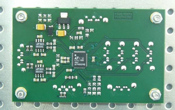
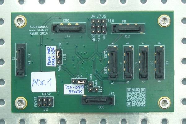
A fast two-channel analog-to-digital converter. Input connector is a differential SATA connector - one for both analog channels. Output connector is a serial-parallel LVDS output to differential SATA connector:
Module interface
Sampling clock
The module requires connecting to a central clock, common to all digitising circuits - they would be derived through clkhub and from lokálního disciplinovaného oscilátoru. Their signal has to be brought to module by SATA cable to ENC SATA connector.
Data output
ADC’s data output assumes an established connection to FPGA, which would carry out the basic signal processing. Because the ADC has an adjustable bit width of output bus, the output connectors are again SATA. They are symmetrically divided in such way, that each receives one bit from every ADC channel.
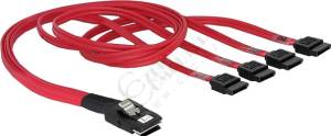
There is also a possibility to connect through miniSAS-SATA cable - its connectors (on SATA side) are divided, according to a required sampling rate and the number of ADC, between individual ADC modules (increasing the bit width of bus lower the required bit speed of connection).
FPGA board thus needs miniSAS connector or several SATA connectors with several aggregated SATA cables.
Module application
One of the intended uses with for a system of ARAS stations which has an unresolved problem of signal digitalisation from the antenna array.
Parameters important for the construction are:
- Dynamic range > 80 dB
- Phase stability between individual channels
- Noise
- Sampling jitter < 100m
Currently, the problem is tackled on a professional level by proprietary digitising units 1) or in more amateur conditions by a system of multichannel sound cards 2)3).
Choice of ADC
Choice of ADC influences a signal format fed into FPGA. There are several formats that are provided by available ADCs:
DDR LVDSJEDEC 204BJESD204AParalel LVDSSerdes- serial LVDS
So far, probably the most perspective is the usage of serial LVDS that requires the smallest number of differential signal pairs, making the whole construction simpler. 4)
If we limit the choice of ADC by a requirement for a serial LVDS output for each ADC channel individually, there will only be a few suitable circuits. Texas Instruments does not produce such fast 16 bit transducers at all and even their slower variants do not have LVDS output. Analog Devices, on the other hand, does not have ADC with serial data output with a bit with of interface smaller than 4bit/channel. We are left with a choice from the company Linear technology: either LTC2271 or products from the LTC2190-2195 series.
As can be seen, the whole ADC series from Linear technology is more or less the same (the converters are even mutually interchangeable between the same PCB layout), they only differ in sampling rates and S/N ratio. The slowest one of them can be used for sampling rate of 20 MHz. The slowest sampling rate that it is able to carried out is 5 MSPS. All converters from this category are more or less configurable and all ADCs’ (even others than made by Linear Technology) have SPI interface for configuration.
Related sites
Refferences
Existing grabbing cards
There are several problems with these devices - especially their high price, unnecessarily high sampling rates and small dynamic range or, on the contrary, large dynamic range, but extremely low sampling rates.


