Table of Contents

(remove this paragraph once the translation is finished)
Rules for designing new modules
This page serves as a wiki complement to an original article Proposed rules and standard procedures. It also serves as a site for placing additional rules of module design, which are not dealt with in the article.
The module design itself uses the following software tools.
Identification of modules
Each module has to carry an unambiguous identification mark consisting of its name, version, and module revision - e.g. JTAGFT2232V02A.
- JTAGFT2232 - the name of the module, depicting the nature of the module (here probably a J-tag programmer with FTDI FT2232 chip).
- (V)02 - the module’s version - there already were some crucial changes during the modules development (in this case, there was CPLD added from version 01)
- A - the module’s revision (in this case there were not corrections of any mistakes)
Furthermore, there are modules with green non-soldering mask and white print and modules with white mask and green print. This kind of module identification was introduced by UST company, which produces modules for MLAB. The meaning of the above-mentioned colour identification is as follows:
- Green mask and white print - a prototype module, often made only in one or few pieces serving as testing samples
- White mask and black print - a production version made in large quantities. Compared to the green version, it may contain tiny changes even if the module’s identification mark is identical.
Creating a new module
Using a GitHub template
The probably simplest way how to make a new module structure is to create a new repository based on the GitHub MLAB module template repository.
The template repository should be used in the standard GitHub way.
Using a mlabgen script
The first step is to create a correct directory structure of a new module in the fork of the main modules' repository. A basic guide for using github.
The directory structure can be created either manually or using a mlabgen tool, which will create the directory structure by itself and correctly name all the files. After its installation, a new module can be created using the following command:
mlabgen-module-init NAMEVERREV
The NAMEVERREV is the new module’s identification created by us. The mlabgen-module-init command has to be executed in the folder, where we want to create the new module. If we plan to create a module with sensor, it has to be placed in the Modules/sensors folder.
Using the mlabgen-module-init command is recommended because the script also creates some additional files - for example an QR code for the new module.
Next step is to edit the metadata file <NAMEVERREV>.json in the directory structure of the module in such way, that it would contain the basic information about the new module. Then we can add the directory structure of the module to the repository. After finishing the module design, it is useful to create a pull-request to the main MLAB repository, which has been forked - this is the best way to make your work visible.
Commit log should be completed with an information that a new module has been added together with its purpose. Further documentation should be already created during the module development. It is therefore useful to create a module’s wiki page here, shorty after the commit of the new module. Creating a page can be done by opening a wiki page from the List of the MLAB modules page.
Manual module creation
If for some reason, you are reluctant to use MLABgen for the creation of the basic directory structure, it is necessary to comply with the following rules:
In the appropriate folder category, we create a folder with the name of the new module using the format of NAMEVERREV. Inside the folder, we create the following directory structure (obligatory folders/files are marked with an asterisk):
<NAMEVERREV>*
├── doc*
│   ├── img*
│   │   ├── <NAMEVERREV>_QRcode.png*
│   │   └── <NAMEVERREV>_top_big.jpg*
│   ├── pdf
│   │   └──
│   ├── <NAMEVERREV>.cs.pdf
│   ├── <NAMEVERREV>.en.pdf
│   └── src
│       └── <NAMEVERREV>.tex
├── hw
│   ├── cam_profi
│   │   ├── <NAMEVERREV>-B.Cu.gbr
│   │   .
│   │   .
│   │   └── <NAMEVERREV>-PTH.drl
│   └── sch_pcb
│       ├── <NAMEVERREV>.kicad_pcb
│       ├── <NAMEVERREV>.pro
│       └── <NAMEVERREV>.sch
├── cad
│   ├── src
│   │   └── <NAMEVERREV>.scad
│   └amf
│       └── <NAMEVERREV>.amf
├── <NAMEVERREV>.json*
└── sw
    └── <NAMEVERREV>_exmalpe.py
The file <NAMEVERREV.json> should contain the information concerning the module.
{
    "wiki": "None",
    "status": "1",
    "name": "<NAMEVERREV>",
    "short_en": “Short  description in English",
    "image": “Picture adress, if not available, use QR code",
    "longname_cs": “Czech subtitle",
    "longname_en": “English subtitle”,
    "mark": "50.0",
    "ust": "",
    "doc_cs": "",
    "short_cs": “Short description in Czech",
    "doc_en": "",
    "root": “folder within the repository",
    "author[]": [],
    "category[]": []
}
You can find an example of a correct filling by checking one of the already existing module.
Module power supply
You can find more detailed examples of connectors and an explanation of their use at Manuals.
MLAB connectors configuration
Power supply connectors for low currents have two configurations (??) which are implemented using .. (??) Napájecí konektory pro nízké proudy mají dvě konfigurace a jsou realizovány lámacími hřebínky s roztečí 2,54mm
Power supply connectors are doubled in order to allow power looping
External power sources
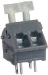
For power supply with higher powers, the FASTON connectors or WAGO256 terminal blocks are used.
There are always openings for WAGO256 terminal block on PCB, because the terminal blocks and FASTON have the same with and it is thus possible to fit both types of connectors onto one PCB.
Cylindrical power supply connector
Power supply +5V from USB
It is always a good practice to include a safety current PTC fuse into the USB power supply in case of modules powered from USB that are able to further distribute the power so that the HOST system is not overloaded.
High voltage
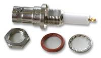
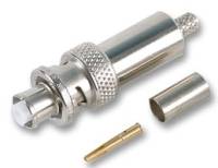
For high voltage distribution (>250V DC) to modules, there are special high-voltage connectors SHV that can be used up to approximately 10kV. SHV connectors, compared to other coaxial connectors, have an advantage that it is not possible to confuse them with the usual measuring BNC connectors.
Due to usually very good insulating parameters of coaxial cables, it is possible to use coaxial cable RG58 for construction of high-voltage distributions.
Safety features
Module schema
A properly drawn schema (not only of MLAB modules) follows these rules:
- Connections cross each other as little as possible
- Signals are led from left to right.
- Positive power supply is led from top to the bottom, negative from bottom to the top.
- A connection cannot cross any text / inscription
- Decoupling capacitors are connected with their positive pole to the place they should decouple (if not possible, they are drawn closely to the decoupled circuit).
- One connection has to contain a minimal amount of connecting points (it is for example not recommended to draw two T nodes, instead it is better to draw one + node).
- Components’ values must have a common name convention using full names of the physical quantities - e.g. nF, pF etc.
A specific feature of MLAB schemes is, that the nails are always in pair, but to keep the scheme intelligible, they are shown as one component (in some cases it requires using own libraries, but on the other hand, schemes are much more intelligible).
Safety resistors
We advice to use safety serial resistors on inputs of some of our modules (e.g. sensors or often modules working at 3.3V) - they will increase the resistance to extreme preload. Size of such resistors is usually within range 10 Ohm to 1 kOhm, with respect to the IO pin’s current requirements.
Safety diodes
Almost all the present MLAB modules contain a safety antiparallel diode on the power supply input, serving as a protection against polarity reversal. It short-circuits the power supply in case of connecting the power voltage of incorrect polarity. In order to function correctly, the diode requires power supplies with current limit.
Therefore it is not recommended to power supply the modules directly from accumulators, as they are able to damage (evaporate) the diode in case of wrong connecting and thus ruin its function. When using modules together with accumulator or battery power supply, we recommend using a proper power supply module that contains a fuse or a converter with current limitation.
Module geometry
Sizes
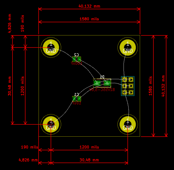
MLAB modules are designed in 10.16 mm raster (400 mils) and their sizes exceed 200 mils - 10 mils from the centers of the corner holes. Each module is 10 mils smaller in size than the exact raster due to production tolerances (otherwise it might not be possible to fit two modules next to each other on a baseboard). To make it possible to fit modules next to each other, it is necessary to make each size smaller by 0.254 mm (10 mils). For mounting on the ALBASE, we use M3 screws of 12 mm in length - that is why it is necessary to have four 3 mm diameter openings on each PCB.
An example of a module occupying 3 openings on the ALBASE:
- Length of the edge: 4×10.16 - 0.254 -0.254 = 40.132 mm
- Screws’ pitch: 3×10.16 = 30.48 mm
- The distance of the screw hole center from the base’s edge: 5.08 - 0.254 = 4.826 mm
- Screw hole diameter: 3 mm (MLAB footprint)
Edge screws
Screws need to have a sufficiently large space around them in order to fasten two contra-nuts that are holding a screw in a module and at the same time serve as a spacer washer between a PCB and a base. PCB is thus placed at the height of two nuts above the base (approx. 5 mm) making the available space for assembly of components 4.9 mm. In case of using larger components, a module can be slightly raised by inserting a required number of washers between both nuts (usually one or two washers are sufficient, otherwise it is recommended using a spacer column or another nut).
Nuts are used thanks to the fact that two nuts make it possible to use a contra-nut effect - they hold firmly and are not released easily compared to simple columns, which have to be secured against release by other ways (e.g. using an anaerobic glue).
Layout (PCB design)
Limits of production possibilities:
Minimal trace width (?? Cesta) 0.1 mm
Minimal insulating space 0.1 mm
Conductive traces (??) in PCB and their sizes are always chosen so even an amateur production and PCB mounting are supported as much as possible. Insulating distance are therefore maximal and spaces for components are chosen to be a bit longer than necessary (especially in case of QFN containers, where such approach makes a soldering quality check much easier).
The traces are furthermore design to minimise the possibility of modules’ emissions - this usually means to minimise the area of knots (?? Smyček), especially in case of boards with alternating currents of high amplitude (e.g. inverters) or in case of outputs of logical circuits of CMOS and TTL types.
In case of two-layer PCBs we prefer to use the upper side of the module (the one away from the base board) as a ground potential (??). If necessary, it is possible to have a low-voltage power supply led also in this side. However, it is quite crucial to avoid leading data or high-frequency signals in the top layer (again, due to possibility of emissions and reduction in the signal integrity).
Modules should have all of the four screws connected with the same potential, even in cases when the module is not using the base board’s ground (if there are not any special construction requirements that would make such practice impossible. An exception is for example eth). This practice helps to reduce emissions from modules, especially in cases of multi-layer PCBs.
Components’ encasements
The preferred encasements for components are those from libraries on github verified by us.
The preferred size of SMD casing is currently 0805 series.
Components’ placement
SMD components are placed only at one side of the board - the one turned towards the base board, if possible (B.Cu layer). A reason for this placement is a greater toughness of the construction, lower radiation and easier mounting in a reflow oven.
Layers
F.Cu - top copper (copper layer on the components’ side) (??)
B.Cu - bottom copper (copper layer on the traces side ?? měděná vrstva ze strany spojů)
F.SilkS - silkscreen (components’ side)
B.SilkS - silkscreen (traces’ side ??) potisk strana spojů
F.Mask -  soldermask (components’ side)
B.Mask - soldermask (traces’ side ??) maska strana spojů
Edge.Cuts - board outline
F.Fab - fabrication layer (components’ side) potisk pro osazování strana součástek
B.Fab - fabrication layer (potisk pro osazování strana spojů
When designing a two-layer PCB, one layer is reserved for grounding and power supply - this layer will be set up as a “Split/Mixed plane” and will have an earth and power supply signals assigned to it. Such setting will allow to automatically end traces of these kinds by a VIA into this layer. It is far better than set up the layer as “copper pour” since in such case the traces are difficult to edit.
VIAs
For usual traces
0.8 mm VIA’s diameter and 0.4 mm diameter for drilling
For power traces, the dimensions of VIAs have to be enlarged depending on the currents, or their number have to be increased.
Limits of production
Minimal circle (?? Okruží) size 0.1 mm (VIA’s diameter = drilling diameter + 0.2 mm)
V případech kde to není nutné nenavrhujeme na této mezi. Prodražuje cenu PCB.
Texty v potisku modulu nesmí překrývat prokovy. (Jinak dojde k nečitelnosti potisku v místě prokovu)
Construction parts
When a module has some free space left of a PCB, it is possible to place a spaces for backup components (usually resistors or condensers in 0850 encasement). During components fitting, it is recommended to use double hřebínek (??) - one raw of pins will be connected to power supply Vcc or ground GND and the opposite pins will lead to backup components, as e.g. ATmegaTQ3201A module. An interesting possibility is to make holes in a PCB at the site of backup components, which will enable an easy control of their presence and furthermore will enable an use of SMD LED.
LED
Modules’ indicator LEDs are preferably designed in a way that they shine through the PCB onto the side turned away from the base board. It can be achieved by placing a LED into a hole in a PCB - such kind of mounting is called “reverse mount” and there exist special SMD diodes especially designed for it.
Classic THT LEDs with through feet (?? Led s průchozími nožičkami) are fitted together with an assembly washer (?? Montážní podložka) that makes the fitting easier and protects the LED against an unnecessary thermal stress and bending. The washer (??) slightly enlarges the diameter of the LED’s base - which must be taken into consideration during a PCB design.
Crystals
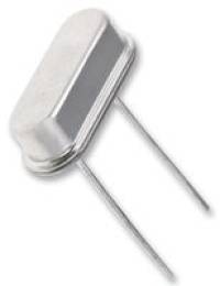
As a basic case for crystals in MLAB modules, we have chosen HC49/S, a small through hole crystal. A reason for this choice was that it can be placed on the top side of the module and its frequency is always visible. Therefore, a constructer always has a good overview about the frequencies used, when working with modules.
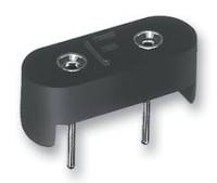
In case of modules, where we assume occasional exchanges of crystals for crystals with other frequencies, we fit them with a special crystal holder. After shortening the legs, crystals can be comfortably inserted into the holder and thus replaced by another crystal any time.
Backup positions for components
Modules’ indicator LEDs can be of SMD or LED 3 mm types. SMD diodes can be placed also on the bottom side of the board that is turned towards the base plate. In such case, it is recommended to design a hole of approximately 1 mm in diameter over the SMD LED, through which the LED will be visible.
Text / Legend printing on modules
Modules’ printings should respect a general typographical rules in order for it to be readable even after an application of screen printing.
Font
One module can accommodate more font sizes (usually less than 3 is necessary). They are used in a following order: name of the module, legend, warnings, author’s id. Different sizes are of course used only in cases, when there is enough space on the module. Some modules have therefore only one font size - with respect to a good readability and module’s size.
Alignment
Same priority signals should have the same font size across the whole module. Size and style of individual legends should also united in case of one connector.
Legend to individual signals on a pin should be aligned to connector in order to minimise a possibility of line error (?? Řádková chubs) when connecting.
Font Sizes
Most commonly used font sizes are as follows:
Width 1.5 mm, Height 1.5mm, Thickness 0.3mm  - module name, important information and pins’ legends
Width 1.3 mm, Height 1.3mm, Thickness 0.3mm  - legend to an individual pin nails (??) popisky jednotlivých vývodů hřebínků
Font sizes smaller than 1.3 mm is problematic and it should only be use when there is a very good reason for it.
Some small modules might have a problem with length of their names - in such cases, the module’s name are wrapped to the next line at module version, for example:
ISL2902001A is the whole module’s name. However, it cannot be placed on the module, that is why it is wrapped at the point of module’s version - ISL29020 and 01A
QR codes
All sufficiently large modules should have a QR code placed on them. It contains module’s identification and a link to a side with module's documentation permalink. QR is generated using a qrencode tool to <modul>/doc/img/<modul>_QRcode.png folder, for example:
qrencode -s 15 -l L "http://www.mlab.cz/" -o "MODUL01A_QRcode.png"
If you have used mlabgen for module generation, QR code should already be created during the creation of the basic directory structure.
It will probably be better to use micro QR codes - qrencode utility is able to generate them (e.g. “qrencode –micro -v 4 -s 15 -l L “BATPOWER04C” -o “microQRcode.png””). However, it still does not exist a suitable reader for Android that will be able to recognise them.
PADS
In order to generate a code for PCB label, Miho created a QR codes generator, which generates ASC formate graphics (originally intended for Mentor Graphics PADS). Size of QR codes on PCBs is so far not unified. When generating codes, the default size is too large for most of PCBs. So far, an acceptable setting has to be tested , e.g.
- PADS Size: 20
- PADS Line Width: 2
The generated file is found at the bottom of the side as a text. The text has to be manually inserted into a file with asc. suffix. After importing the generated picture into a PCB’s printing, its attribute has to be set as “solid copper” so that the motive will be entirely filled in with colour.
KiCAD
QRcode pictures can be added to KiCAD in the same way as logo.
Check list before production
- check if the encasements are right and of a good size
- check the size of connector’s spaces (??ploška) and sizes of components that go through the board
- check the sizes of holes, LED crystals, pins (hřebík??), jumpers (?? Propojka) or other special components
- check the unmasking of (??) plošek and jumpers (??)
- check the components’ outlines and labelling of jumpers (??)
- check the labels and legends, www.mlab.cz title
- check that the VIAs are not under letters and symbols
- check the QR code and PermaLink
MLAB repository structure
- Project metadata - json
- Commit message - begins with capital latter; uses words such as: added, fixed, removed, started, finished…
Name convention
withouth_diacritic_and_special_cases_spaces_are_replaced_by_an_underscore_lowercase_letters_only_briefly_and_comprehensibly
Modules’ directory structure
MODUL01A/
  hw/
    sch_pcb
      gerb_ama
      gerb_profi
    hdl
    cad
  sw/
  doc/
    src
      img
    datasheets
    MODUL01A.cs.pdf
    MODUL01A.en.pdf


